Research
- HOME
- About us
- Research
Soft nanoimprinting
lithography(s-NIL) process
Ultra-flexible electronics
Low-temperature activation process
Soft nanoimprinting lithography(s-NIL) process
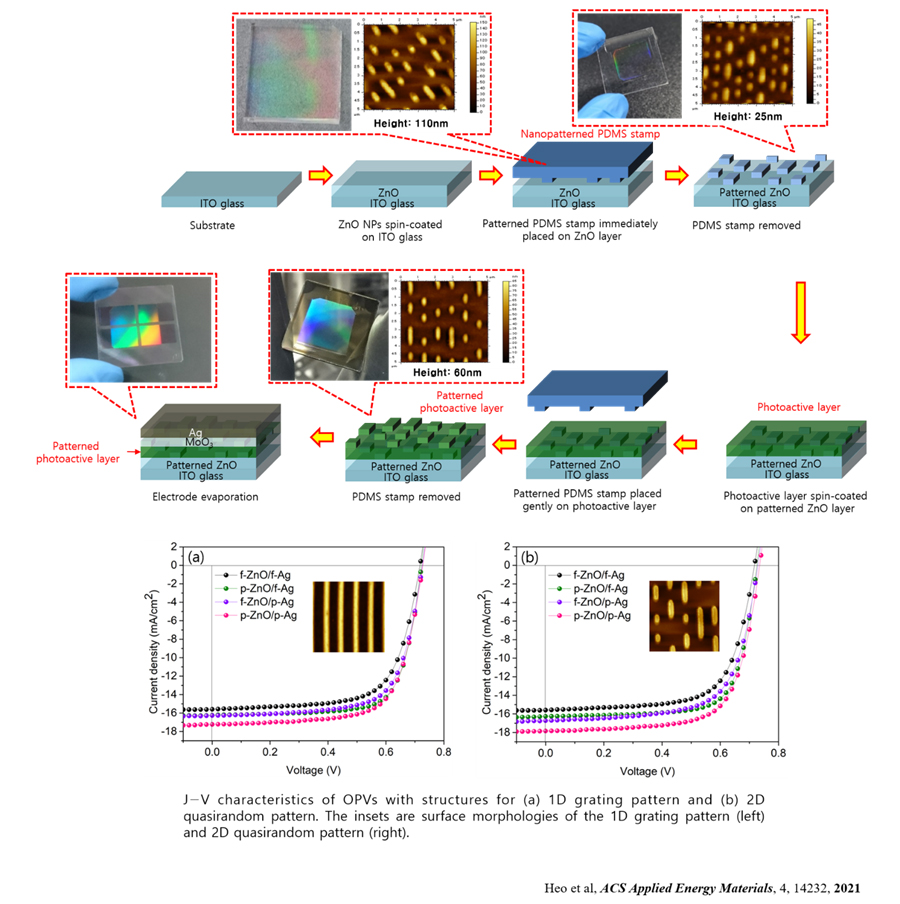
We have s-NIL process technology that can introduce nanostructures onto organic/inorganic layers in organic/inorganic electronics. This technology includes various ink formulation technologies, and it is possible to respond to large-area device fabrication by enabling patterning at room temperature without applying pressure.
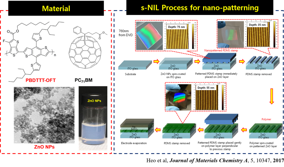
Applying the above technology is expected to improve the light emission properties in OLEDs and the light absorption characteristics in OPVs. In particular, by adjusting the shape or duty cycle of the pattern, it is possible to control the absorption wavelength range of light, so that photon energy can be maximally absorbed.
Patterned photoactive layers with various pattern pitches
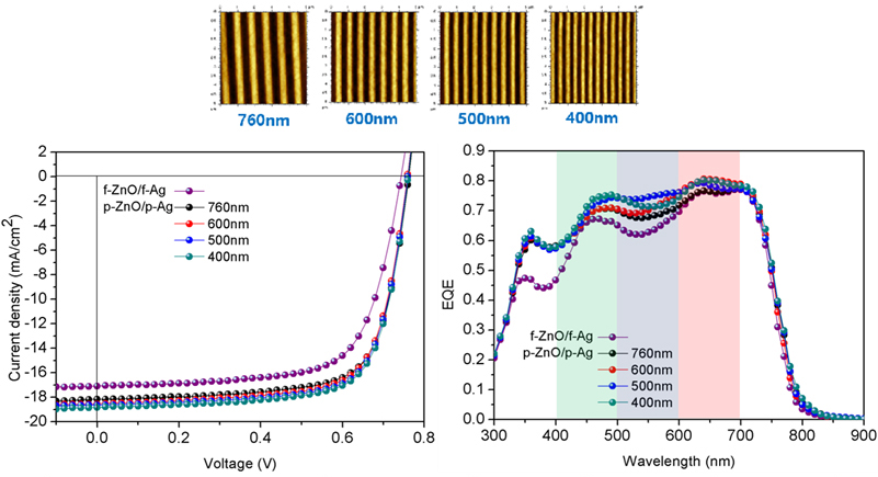
| JSC (mA/cm2) | Voc (V) | FF (%) | PCE (%) | ||
|---|---|---|---|---|---|
| p-ZnO/p-Ag | 760nm | 18.16 (0.06) | 0.76 | 71.7 (0.3) | 9.92 (0.02) |
| 600nm | 18.54 (0.08) | 0.76 | 71.4 (0.4) | 10.05 (0.06) | |
| 500nm | 18.63 (0.07) | 0.76 | 72.3 (0.03) | 10.23 (0.04) | |
| 400m | 18.84 (0.07) | 0.76 | 72.1 (0.03) | 10.33 (0.04) | |
| p-ZnO/f-Ag | 17.64 (0.10) | 0.75 | 72.1 (0.5) | 9.59 (0.11) | |
| f-ZnO/f-Ag | 17.09 (0.05) | 0.75 | 69.0 (0.7) | 8.85 (0.14) | |

Introduction of 2D quasi-random structure for TM/TE balancing